 |
| December 11, 2018 | Volume 14 Issue 46 |
Designfax weekly eMagazine

Archives
Partners
Manufacturing Center
Product Spotlight
Modern Applications News
Metalworking Ideas For
Today's Job Shops
Tooling and Production
Strategies for large
metalworking plants
Metal 3D printing: X-rays, infrared used to find what causes defects
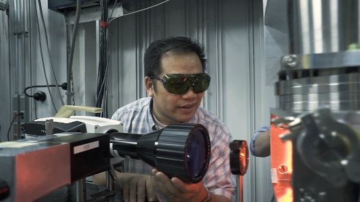
Tao Sun, an X-ray physicist at the US DOE's Argonne National Laboratory lines up an infrared camera, the first to be installed at an X-ray synchrotron source. This provides 3D images of the printing process in nearly real time to benchmark a printing process. Calibrating the X-ray results to the IR camera allows for the use of IR cameras to detect defects in processing on manufacturing lines. [Image by Argonne National Laboratory.]
By Tao Sun, physicist and X-ray scientist, Argonne National Laboratory
Additive manufacturing (AM), or three-dimensional (3D) printing, has given product designers and engineers considerable freedom -- the freedom to design custom, intricate parts and to produce them very, very quickly. This freedom has made AM techniques common and useful tools for rapid prototyping. Application of these techniques may soon widen, however, thanks to recent advances in computing and to the explosion of materials for and access to 3D-printing technologies.
In light of these changes, AM now has the potential to be used for large-scale, rapid production of parts with complex geometries. This potential could reinvigorate aerospace, defense, transportation, and numerous other industries by shortening development cycles.
While the potential to grow 3D-printing applications exists, numerous hurdles still stand in the way. The formation of defects within materials is one example; defects undermine the reproducibility of parts and generate unnecessary waste in the process. But our understanding of how and why these defects form, and what it takes to minimize them, remains limited, in turn limiting the ability to grow AM applications.
To overcome such hurdles, researchers at the U.S. Department of Energy's (DOE) Argonne National Laboratory are taking on a lead role. In collaboration with industry, universities, and government institutions, Argonne researchers are investigating the fundamental physics that underlie AM processes by leveraging laboratory capabilities. Their work focuses on powder bed fusion of metal powders -- an AM technique using lasers to fuse metal powders layer by layer.
Argonne's Advanced Photon Source (APS), a DOE user facility and one of the world's brightest sources of high-energy X-ray beams, is home base for this research. Here, researchers have mounted a metal laser-printing simulator and high-speed infrared camera onto one of the APS's X-ray beamlines. Together, these tools enable researchers to visualize the 3D-printing process in real time and gather insightful data that can, when analyzed, fill in gaps in our understanding of AM processes and spark ideas for improvement.
Video: New additive manufacturing research tool mimics manufacturing process
We integrated X-ray and infrared imaging because they go hand in hand. Each gives us different kinds of information that complements the other. X-ray imaging provides information about the dynamics of the microstructures, and infrared imaging provides details about thermal processes.
Why X-ray imaging
The APS is a rare source for ultra-bright high-energy X-rays. With a beamline dedicated to AM and an array of in-situ scattering and diffraction tools, users can snapshot the 3D-printing process at the lighting fast rate of 6.5 million frames per second. They can analyze the X-ray imaging and diffraction data to address unresolved questions about the solidification, melting, vaporization, and porosity of different materials under extreme thermal conditions. Analysis and characterization tools also enable users to study conditions like stress and corrosion, as well as processes like phase evolution and texture development in situ.
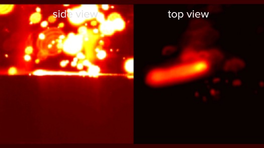
Infrared and X-ray imaging of the 3D printing of a metal part can help scientists better understand the 3D-printing process so they can benchmark processes and materials to reduce defects. [Image by Argonne National Laboratory.]
Argonne researchers, in collaboration with researchers from the Missouri University of Science and Technology, DOE's Kansas City National Security Campus, Carnegie Mellon University, and Northwestern University, harnessed the powerful resources of the APS to capture the formation of microscopic defects during 3D laser printing of metals. Visualizing the process using X-ray imaging and diffraction, researchers generated a movie that shows how microscopic structures of the sample changed as the laser came in contact. They were also able to quantify various 3D-printing characteristics, including the size and shape of the melt pool, spattering behaviors, solidification velocity, and phase transformation rate.
A forthcoming upgrade of the APS will allow its beamlines produce even brighter and more focused X-rays. This could enable researchers to visualize AM processes more clearly and in even greater detail.
Why infrared imaging
Infrared cameras deliver useful information about thermal processes across a surface. This kind of information is valuable to a field like AM in which heat and heat transfer are fundamental to the formation of products, yet remain poorly understood. By pairing X-ray imaging with infrared imaging, Argonne researchers aim to help manufacturers and researchers alike better understand these complex phenomena and their impact on the properties of finished products.
Argonne is the first to integrate both a 3D-printing apparatus and a high-speed infrared camera onto an X-ray beamline at a high-energy synchrotron. The combination of the infrared temperature-monitoring system and top-of-the-line X-ray imaging delivers unprecedented details about materials dynamics.
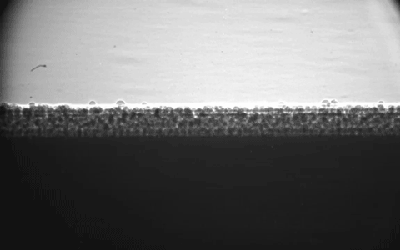
The Advanced Photon Source generates high-energy X-rays that show 3D printing in near real time. [Image by Argonne National Laboratory.]
With the high-speed infrared camera at the APS, scientists can capture thermal details at a rate of 95,000 frames per second while the 3D-printing process is underway. Information from the infrared camera supports analysis of the heating and cooling rates, visualization of the formation of defects, and the evaluation of post-production components.
One way infrared imaging can support AM research is by helping researchers visualize the formation of plumes that emerge when a metal powder vaporizes after coming into contact with the laser. These plumes, which can impact laser absorption, are not visible using X-rays alone, but can be captured through infrared imaging. Learning more about them can help manufacturers understand phenomena, such as spattering and melt pool fluctuation, in order to come up with means of controlling their own systems to minimize disruption.
In addition to being useful for analyses at the APS, infrared cameras -- unlike like synchrotron light sources -- are readily available to manufacturers and system owners worldwide. Thus, by integrating an infrared camera onto the beamline at the APS, Argonne has created a window for outside users to connect with the data and insights being generated at the synchrotron facility.
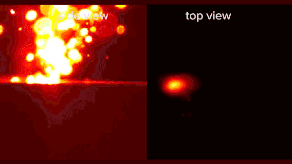
Together, infrared and X-ray imaging can help scientists better understand the 3D-printing process. [Image by Argonne National Laboratory.]
Aaron Greco, material scientist and co-project leader of the AM effort at the laboratory, says this development could, in the future, help users leverage APS insights to improve their own systems. For example, if X-ray and infrared imaging help researchers identify a thermal signature correlated to the formation of defects, real-world system owners could potentially exploit that information to mitigate defects in their own systems. The addition of our infrared camera helps us form those early foundational links between the basic science we do here and the applied science being done out in the world.
Modeling and simulation
Detailed data from X-ray and infrared imaging can also advance AM by improving models of printed materials and AM processes. Better models deliver more reliable predictions, with which manufacturers can optimize processing parameters and material designs.
Better predictive models can not only accelerate the optimization of new materials and processes, they can also help minimize traditional trial-and-error prototyping during development, which can be costly and time consuming. Developing such models of complex processes, however, often demands significant computational power and expertise, which many manufacturers lack. Manufacturers are further limited by the extremely detailed models currently in the marketplace, which have limited flexibility and applications.
Argonne capabilities can address many of these problems. In addition to its expertise in discovering, characterizing, and scaling up materials, the laboratory is rich in computational tools for collecting and analyzing data. The laboratory also boasts experts in modeling and machine learning who can help create more flexible, faster-running models more suited to industry needs.
Some of these resources and experts can be found at Argonne's Laboratory Computing Resource Center. The center operates Bebop, a 1040-node computing cluster, and Blues, a 780-node computing cluster, as production systems and software development platforms. These systems can undertake complex problems that are computationally expensive, including efficiently run molecular dynamics and kinetic Monte Carlo simulations, among other things.
Other resources can be found at the Argonne Leadership Computing Facility (ALCF), an DOE Office of Science User Facility that operates computing resources that are 10 to 100 times more powerful than systems typically used for scientific research. ALCF resources include Theta, an 11.69-petaflop supercomputer, and will soon include Aurora, set to be the nation's first exascale system upon its expected 2021 arrival.
Argonne's wide repertoire of imaging and computational resources can deliver the knowledge needed to fully comprehend how AM processes work and how they can be improved. Experts at Argonne already support researchers from industry and academia in characterizing material samples under in-situ conditions and in developing models and simulations of material interactions at a very high fidelity.
Ultimately, our goal is to give industry the deeper level of understanding needed to improve AM processes. By aligning our computing with our advanced manufacturing expertise, we can build on this goal and further grow U.S. manufacturing.
The infrared camera is located at the APS's 32-ID-B beamline. The camera was funded through Argonne's Laboratory Directed Research Development program as part of the laboratory's Manufacturing Science and Engineering program.
Published December 2018
Rate this article
View our terms of use and privacy policy